- 您现在的位置:买卖IC网 > Sheet目录1998 > ICS843156AKILF (IDT, Integrated Device Technology Inc)IC CLK GENERATOR 32VFQFP
ICS843156AKI REVISION B NOVEMBER 28, 2012
11
2012 Integrated Device Technology, Inc.
ICS843156I Data Sheet
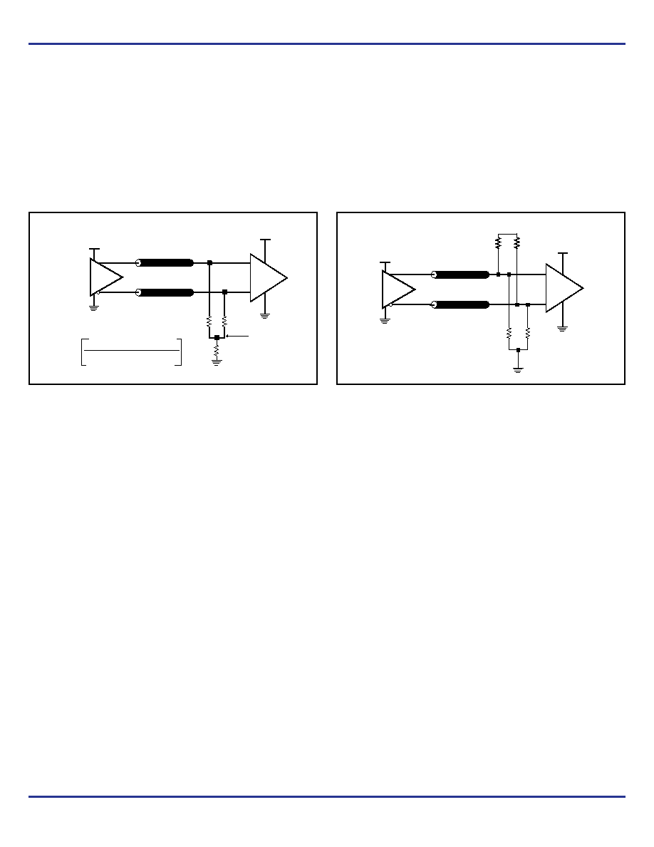
CRYSTAL-TO-LVPECL CLOCK SYNTHESIZER
Termination for 3.3V LVPECL Outputs
The clock layout topology shown below is a typical termination for
LVPECL outputs. The two different layouts mentioned are
recommended only as guidelines.
The differential outputs are low impedance follower outputs that
generate ECL/LVPECL compatible outputs. Therefore, terminating
resistors (DC current path to ground) or current sources must be
used for functionality. These outputs are designed to drive 50
transmission lines. Matched impedance techniques should be used
to maximize operating frequency and minimize signal distortion.
Figures 4A and 4B show two different layouts which are
recommended only as guidelines. Other suitable clock layouts may
exist and it would be recommended that the board designers
simulate to guarantee compatibility across all printed circuit and clock
component process variations.
Figure 4A. 3.3V LVPECL Output Termination
Figure 4B. 3.3V LVPECL Output Termination
3.3V
V
CC - 2V
R1
50
Ω
R2
50
Ω
RTT
Z
o = 50Ω
Z
o = 50Ω
+
_
RTT =
* Z
o
1
((V
OH + VOL) / (VCC – 2)) – 2
3.3V
LVPECL
Input
R1
84
Ω
R2
84
Ω
3.3V
R3
125
Ω
R4
125
Ω
Z
o = 50Ω
Z
o = 50Ω
LVPECL
Input
3.3V
+
_
发布紧急采购,3分钟左右您将得到回复。
相关PDF资料
ICS843156AKLF
IC CLK GENERATOR 32VFQFP
ICS843202AYILF
IC SYNTHESIZER 680MHZ 32-LQFP
ICS843204AGILF
IC SYNTHESIZER LVPECL 48-TSSOP
ICS84320AY-01LN
IC SYNTHESIZER GP LVPECL 32-LQFP
ICS84320AYI-01LF
IC FREQ SYNTHESIZER 32TQFP
ICS843251AG-04LF
IC CLK GENERATOR LVPECL 8-TSSOP
ICS843251AGI-14LF
IC CLK GEN ETHERNET 25MHZ 8TSSOP
ICS843251BGI-12LF
IC CLK GENERATOR LVPECL 8-TSSOP
相关代理商/技术参数
ICS843156AKILFT
功能描述:IC CLK GENERATOR 32VFQFP RoHS:是 类别:集成电路 (IC) >> 时钟/计时 - 时钟发生器,PLL,频率合成器 系列:HiPerClockS™ 标准包装:1,000 系列:- 类型:时钟/频率合成器,扇出分配 PLL:- 输入:- 输出:- 电路数:- 比率 - 输入:输出:- 差分 - 输入:输出:- 频率 - 最大:- 除法器/乘法器:- 电源电压:- 工作温度:- 安装类型:表面贴装 封装/外壳:56-VFQFN 裸露焊盘 供应商设备封装:56-VFQFP-EP(8x8) 包装:带卷 (TR) 其它名称:844S012AKI-01LFT
ICS843156AKLF
功能描述:IC CLK GENERATOR 32VFQFP RoHS:是 类别:集成电路 (IC) >> 时钟/计时 - 时钟发生器,PLL,频率合成器 系列:HiPerClockS™ 标准包装:1,000 系列:- 类型:时钟/频率合成器,扇出分配 PLL:- 输入:- 输出:- 电路数:- 比率 - 输入:输出:- 差分 - 输入:输出:- 频率 - 最大:- 除法器/乘法器:- 电源电压:- 工作温度:- 安装类型:表面贴装 封装/外壳:56-VFQFN 裸露焊盘 供应商设备封装:56-VFQFP-EP(8x8) 包装:带卷 (TR) 其它名称:844S012AKI-01LFT
ICS843156AKLFT
功能描述:IC CLK GENERATOR 32VFQFP RoHS:是 类别:集成电路 (IC) >> 时钟/计时 - 时钟发生器,PLL,频率合成器 系列:HiPerClockS™ 标准包装:1,000 系列:- 类型:时钟/频率合成器,扇出分配 PLL:- 输入:- 输出:- 电路数:- 比率 - 输入:输出:- 差分 - 输入:输出:- 频率 - 最大:- 除法器/乘法器:- 电源电压:- 工作温度:- 安装类型:表面贴装 封装/外壳:56-VFQFN 裸露焊盘 供应商设备封装:56-VFQFP-EP(8x8) 包装:带卷 (TR) 其它名称:844S012AKI-01LFT
ICS8431AM-21
制造商:ICS 制造商全称:ICS 功能描述:350MHZ, LOW JITTER, CRYSTAL OSCILLATOR-TO-3.3V LVPECL FREQUENCY SYNTHESIZER
ICS8431AM-21LF
功能描述:IC SYNTHESIZER GP LVPECL 28-SOIC RoHS:是 类别:集成电路 (IC) >> 时钟/计时 - 时钟发生器,PLL,频率合成器 系列:HiPerClockS™ 标准包装:1,000 系列:Precision Edge® 类型:时钟/频率合成器 PLL:无 输入:CML,PECL 输出:CML 电路数:1 比率 - 输入:输出:2:1 差分 - 输入:输出:是/是 频率 - 最大:10.7GHz 除法器/乘法器:无/无 电源电压:2.375 V ~ 3.6 V 工作温度:-40°C ~ 85°C 安装类型:表面贴装 封装/外壳:16-VFQFN 裸露焊盘,16-MLF? 供应商设备封装:16-MLF?(3x3) 包装:带卷 (TR) 其它名称:SY58052UMGTRSY58052UMGTR-ND
ICS8431AM-21LFT
功能描述:IC SYNTHESIZER 350MHZ 28-SOIC RoHS:是 类别:集成电路 (IC) >> 时钟/计时 - 时钟发生器,PLL,频率合成器 系列:HiPerClockS™ 标准包装:1,000 系列:- 类型:时钟/频率合成器,扇出分配 PLL:- 输入:- 输出:- 电路数:- 比率 - 输入:输出:- 差分 - 输入:输出:- 频率 - 最大:- 除法器/乘法器:- 电源电压:- 工作温度:- 安装类型:表面贴装 封装/外壳:56-VFQFN 裸露焊盘 供应商设备封装:56-VFQFP-EP(8x8) 包装:带卷 (TR) 其它名称:844S012AKI-01LFT
ICS8431AM-21T
制造商:ICS 制造商全称:ICS 功能描述:350MHZ, LOW JITTER, CRYSTAL OSCILLATOR-TO-3.3V LVPECL FREQUENCY SYNTHESIZER
ICS8431AMI-21
制造商:ICS 制造商全称:ICS 功能描述:350MHZ, LOW JITTER, CRYSTAL OSCILLATOR-TO-3.3V LVPECL FREQUENCY SYNTHESIZER